By Muhammad Ibrahim · Published October 27, 2026 · 8 min read
Full Adder Circuit with 7486, 7408 and 7432: Truth Table and Pin-by-Pin Wiring
The general theory of the full adder is already covered in the half adder and full adder tutorial on this site, so this page is about the actual Lab 4 build: every connection, a quick way to check all eight rows, and what to look at when one row is wrong. The circuit has three inputs, A, B and the carry-in (my switch C), and two outputs, SUM and CAR (the carry-out). It uses only five gates on three chips.
- CHIPS
- 7486, 7408, 7432
- GATES USED
- 5 (2 XOR, 2 AND, 1 OR)
- INPUTS
- 3 switches (A, B, C)
- OUTPUTS
- 2 LEDs (SUM, CAR)
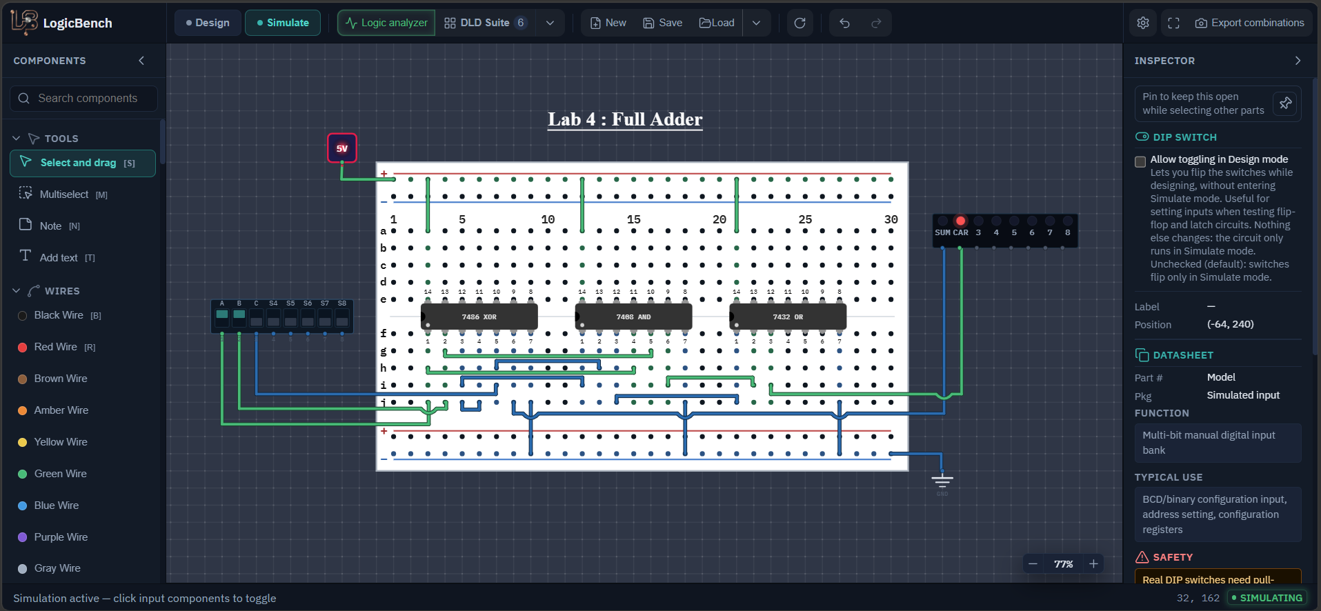
Components needed for the full adder
- A 7486 (quad XOR), a 7408 (quad AND) and a 7432 (quad OR)
- A DIP switch with three switches in use, renamed A, B and C (C is the carry-in)
- A Light Bar with two LEDs in use, renamed SUM and CAR
- A Regulated +5V Power part, a Ground (GND) part and one half-size breadboard
Open the circuit
Open the exact full adder from the lab. Switch to Simulate, set A, B and C, and read the SUM and CAR LEDs.
Full adder circuit diagram
P = A⊕B is created once and used in three places: the second XOR, and the P·C gate. Small numbers are chip pin numbers.
How to build a full adder with XOR, AND and OR gates
Place the three chips and power them
Put the 7486, 7408 and 7432 on the breadboard. Connect pin 14 of each chip to +5 V and pin 7 of each chip to ground. Check this now, because a chip without power looks exactly like a logic mistake later.
First XOR: A with B
On the 7486 connect A to pin 1 and B to pin 2. The output on pin 3 is A⊕B. I will call this signal P, because it decides whether an incoming carry gets passed on (more on that in the theory section). P is used in three places, so be ready to connect it to three pins.
Second XOR makes the SUM
Still on the 7486, connect P (pin 3) to pin 4 and connect C to pin 5. The output on pin 6 is P⊕C, which equals A⊕B⊕C. Connect pin 6 to the SUM LED.
Make the two carry terms with the 7408
First AND gate: connect P to pin 1 and C to pin 2. Pin 3 is then P·C. Second AND gate: connect A to pin 4 and B to pin 5. Pin 6 is then AB. These are the only two ways a carry can be produced, and they are explained below.
Combine them into the carry-out
On the 7432 connect pin 1 to pin 3 of the 7408 (P·C) and pin 2 to pin 6 of the 7408 (AB). The output on pin 3 is the carry-out. Connect it to the CAR LED.
Check all eight rows with a shortcut
Switch to Simulate. For every combination of A, B and C the two LEDs, read as a binary number with CAR first and SUM second, must equal the number of switches that are on. In other words SUM + 2 × CAR = A + B + C. If that holds for all eight rows, the adder is correct. Export combinations in the toolbar will save an image of every row if you need them for your report.
Full adder pin connections
| Signal | Connects to | Meaning |
|---|---|---|
| A | 7486 pin 1 and 7408 pin 4 | Input A |
| B | 7486 pin 2 and 7408 pin 5 | Input B |
| C | 7486 pin 5 and 7408 pin 2 | Carry-in |
| 7486 pin 3 | 7486 pin 4 and 7408 pin 1 | P = A⊕B, used three times |
| 7486 pin 6 | SUM LED | SUM = P⊕C |
| 7408 pin 3 | 7432 pin 1 | P·C |
| 7408 pin 6 | 7432 pin 2 | AB |
| 7432 pin 3 | CAR LED | Carry-out = P·C + AB |
Full adder truth table
| A | B | C | SUM | CAR | A + B + C |
|---|---|---|---|---|---|
| 0 | 0 | 0 | 0 | 0 | 0 |
| 0 | 0 | 1 | 1 | 0 | 1 |
| 0 | 1 | 0 | 1 | 0 | 1 |
| 0 | 1 | 1 | 0 | 1 | 2 |
| 1 | 0 | 0 | 1 | 0 | 1 |
| 1 | 0 | 1 | 0 | 1 | 2 |
| 1 | 1 | 0 | 0 | 1 | 2 |
| 1 | 1 | 1 | 1 | 1 | 3 |
Generate and propagate signals inside the full adder
When one row is wrong, find the first column here that does not match what you see on the wire.
| A | B | C | P = A⊕B | P·C | AB | CAR |
|---|---|---|---|---|---|---|
| 0 | 0 | 0 | 0 | 0 | 0 | 0 |
| 0 | 0 | 1 | 0 | 0 | 0 | 0 |
| 0 | 1 | 0 | 1 | 0 | 0 | 0 |
| 0 | 1 | 1 | 1 | 1 | 0 | 1 |
| 1 | 0 | 0 | 1 | 0 | 0 | 0 |
| 1 | 0 | 1 | 1 | 1 | 0 | 1 |
| 1 | 1 | 0 | 0 | 0 | 1 | 1 |
| 1 | 1 | 1 | 0 | 0 | 1 | 1 |
How the full adder works: generate and propagate
Generate and propagate
A stage produces a carry in two different ways. If A and B are both 1 it generates a carry by itself, that is the term AB. If exactly one of A and B is 1, it passes an incoming carry through, that is the term (A⊕B)·C. So the carry-out is AB + (A⊕B)·C. The names are generate (G = AB) and propagate (P = A⊕B), and the equation is Cout = G + P·Cin. The circuit builds exactly this, which is why P is the first signal you create. Carry-lookahead adders are built from the same two signals.
Why the OR gate never double counts
If AB is 1 then A and B are both 1, so A⊕B is 0 and the other term must be 0. The two carry terms are never on together. You can see it in the table of internal signals: at 110 and 111 only AB is 1, and at 011 and 101 only P·C is 1. This is why a plain OR is enough to combine them.
Chaining stages into a 4-bit adder
Connect the carry-out of one stage to the carry-in of the next and you have a ripple-carry adder. With the maximum delays in the LogicBench datasheet entries, the carry path through one stage is an AND (15 ns) and an OR (15 ns), so about 30 ns per stage after the first. The first stage also has the XOR in front of it, which is 23 + 15 + 15 = 53 ns. A 4-bit adder can therefore need around 140 ns (53 + 3 × 30) before the last carry settles, and longer words get slower in the same proportion. That is the reason the real 7483 4-bit adder uses carry-lookahead inside one chip instead of just rippling.
Chip budget
The adder needs 2 XOR, 2 AND and 1 OR gates, which is 5 gates. On the chips that means 2 of the 4 gates on the 7486, 2 of the 4 on the 7408 and 1 of the 4 on the 7432, so seven gates on the board stay unused. That is normal when you build with small-scale chips.
Expected full adder output
- SUM + 2 × CAR equals the number of switches that are on, in all eight rows.
- CAR is on for 011, 101, 110 and 111 only, which are the rows with at least two inputs on.
- At 111 both LEDs are on, because 1 + 1 + 1 = 3 and 3 is 11 in binary.
- SUM is on for 001, 010, 100 and 111, the rows with an odd number of inputs on.
Full adder not working? Common mistakes
CAR is wrong only at 011 and 101
The P·C gate is getting A (or B) where it should get P. Pin 1 of the first AND gate must come from pin 3 of the 7486, the same wire that feeds the second XOR gate.
CAR is wrong only at 110 and 111
The AB gate is missing or its inputs are wrong. Check that A is on pin 4 and B is on pin 5 of the 7408 and that pin 6 reaches pin 2 of the 7432.
SUM is wrong in every row where C is on
The second XOR gate is probably getting A or B in place of P. Pin 4 of the 7486 must be connected to pin 3, and C must be on pin 5.
SUM is right but CAR never lights
The 7432 is a separate chip. Check its pin 14 and pin 7 and check that both of its inputs are really connected to the two AND outputs.
Frequently asked questions
What are the Boolean expressions for a full adder?
SUM = A ⊕ B ⊕ Cin and Cout = AB + Cin(A ⊕ B), which is the same as AB + BCin + ACin. Cout is 1 whenever at least two of the three inputs are 1.
How many gates does a full adder need?
This build uses five: two XOR gates, two AND gates and one OR gate, spread over a 7486, a 7408 and a 7432.
How do you check a full adder without writing the truth table?
Read the two outputs as a binary number with Cout first and SUM second. That number must equal A + B + Cin for every input combination, for example 1 + 1 + 1 = 3 = 11 in binary.
How do you build a 4-bit adder from full adders?
Use four full adders and connect the Cout of each one to the Cin of the next. The first Cin is tied to 0. This is a ripple-carry adder, and the carry has to pass through every stage, so longer adders get slower.
What are generate and propagate in an adder?
Generate (G = AB) means a stage makes a carry on its own, and propagate (P = A⊕B) means it passes an incoming carry through. The carry-out is G + P·Cin, and carry-lookahead adders are built from these two signals.
Try it yourself
Open LogicBench and follow along — the simulator is free and needs no account.
Launch the simulator